Precision Energy Supply of Lithography High-Voltage Supplies in Nanoscale Multi-Patterning Processes
Lithography transfers the circuit patterns onto the wafers, and the multi-patterning processes create the features at the nanoscale through the multiple exposure and the etching steps. The light source of the lithography system provides the exposure energy, and the high-voltage supply of the source controls the energy delivery. The precision energy supply supports the pattern fidelity in the nanoscale processes, and the engineering work covers the energy control, the synchronization, and the verification.
The multi-patterning processes split the dense patterns into the multiple exposure steps, and the alignment and the overlay of the steps determine the final pattern accuracy. The exposure energy affects the line width and the pattern profile, and the stability of the energy is essential for the consistent patterning. The precision supply maintains the energy at the target values.
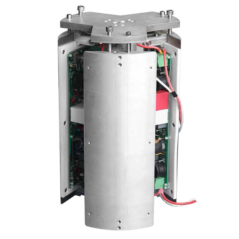
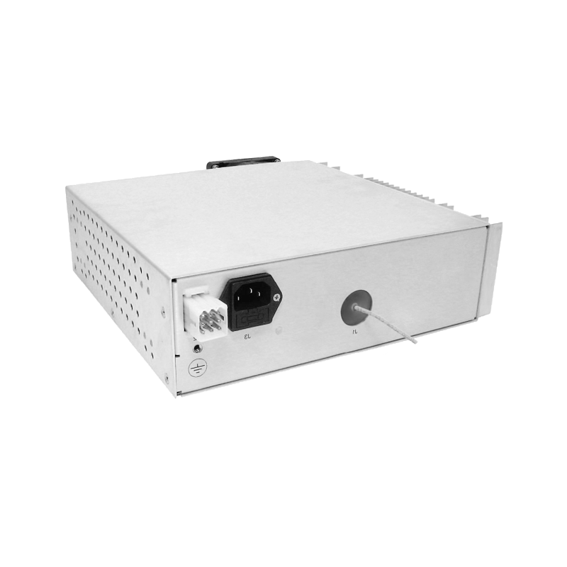
The light source of the lithography system generates the exposure pulses, and the high-voltage supply charges the discharge circuit for the pulse generation. The energy of each pulse is controlled through the charging voltage, and the pulse-to-pulse stability affects the exposure uniformity. The regulation of the supply output is designed for the precision energy delivery.
The synchronization of the exposure with the wafer stage movement is implemented through the control system, and the pulse timing is coordinated with the scanning motion. The energy delivery is synchronized with the exposure positions, and the timing errors are minimized. The synchronization supports the accurate pattern transfer.
The multi-patterning processes require the consistent exposure across the multiple layers, and the energy calibration is performed for the process control. The dose is monitored and corrected for the drift, and the calibration data supports the overlay control. The precision of the energy delivery contributes to the pattern fidelity.
The environment of the lithography cleanroom is controlled for the temperature and the humidity, and the supply is designed for the stable operation in the cleanroom conditions. The cooling of the supply and the source is managed for the thermal stability, and the interference from the other equipment is minimized. The environmental control supports the precision operation.
The monitoring of the exposure process includes the measurement of the energy and the focus, and the process data is used for the control and the analysis. The deviations from the target are detected and corrected, and the process stability is maintained. The monitoring supports the quality of the patterning.
The verification of the supply includes the measurement of the energy stability and the pulse characteristics, and the results are compared with the specification. The long-term stability is verified through the endurance tests, and the synchronization accuracy is measured. The verification supports the qualification of the supply.
The nanoscale patterning is used for the advanced semiconductor manufacturing, and the precision of the exposure determines the device performance. The reliable energy supply supports the production of the fine patterns, and the technology contributes to the advancement of the semiconductor industry.
The advancement of the lithography technology demands the higher resolution and the tighter control, and the supply design follows the requirements of the new processes. The improved control and the higher stability enhance the precision, and the cooperation with the lithography equipment manufacturers drives the innovation.
Precision energy supply of the lithography high-voltage supplies enables the nanoscale multi-patterning processes, and the accurate energy control, the careful synchronization, and the verification deliver the required pattern fidelity. The continued development will support the advancement of the nanoscale semiconductor manufacturing.
The overlay control of the multi-patterning processes requires the precise alignment of the layers, and the alignment marks are measured for the overlay correction. The exposure energy and the focus are optimized for the overlay performance, and the process is monitored for the stability. The overlay control contributes to the accuracy of the nanoscale patterning.
The maintenance of the lithography supply includes the inspection of the discharge components and the verification of the energy calibration, and the condition of the components affects the energy delivery. The replacement of the consumables is scheduled according to the operating hours, and the supply is requalified after the maintenance. The maintenance program supports the reliable production.
The training of the process engineers covers the operation of the lithography system and the interpretation of the exposure data, and the understanding of the energy control supports the process development. The collaboration between the equipment and the process teams improves the integration, and the knowledge sharing supports the continuous improvement.
The evaluation of the patterned wafers includes the measurement of the critical dimensions and the inspection of the pattern defects, and the results are compared with the specifications. The correlation between the exposure conditions and the pattern quality is analyzed, and the process is refined. The evaluation supports the qualification of the multi-patterning process.
The documentation of the lithography process includes the exposure parameters, the calibration records, and the quality data, and the documentation supports the reproducibility and the traceability of the patterning. The reviews of the process data support the improvement, and the documentation is maintained according to the quality system. The documentation supports the production control.
The collaboration between the lithography equipment suppliers and the semiconductor manufacturers supports the development of the advanced patterning processes, and the exchange of the experience contributes to the optimization of the exposure control. The requirements of the new device generations guide the development, and the equipment is adapted for the applications. The collaboration drives the advancement of the semiconductor manufacturing.
The continuous improvement of the patterning process is supported by the data analysis and the experimental validation, and the process changes are implemented after the verification. The performance targets are reviewed periodically, and the improvements are documented. The continuous improvement maintains the competitiveness of the manufacturing process.
The supply of the lithography system is qualified for the production use through the comprehensive verification, and the long-term data from the production confirms the reliability. The performance is maintained over the operating life through the calibration and the maintenance, and the production support provides the assistance. The qualification supports the dependable operation of the manufacturing line.