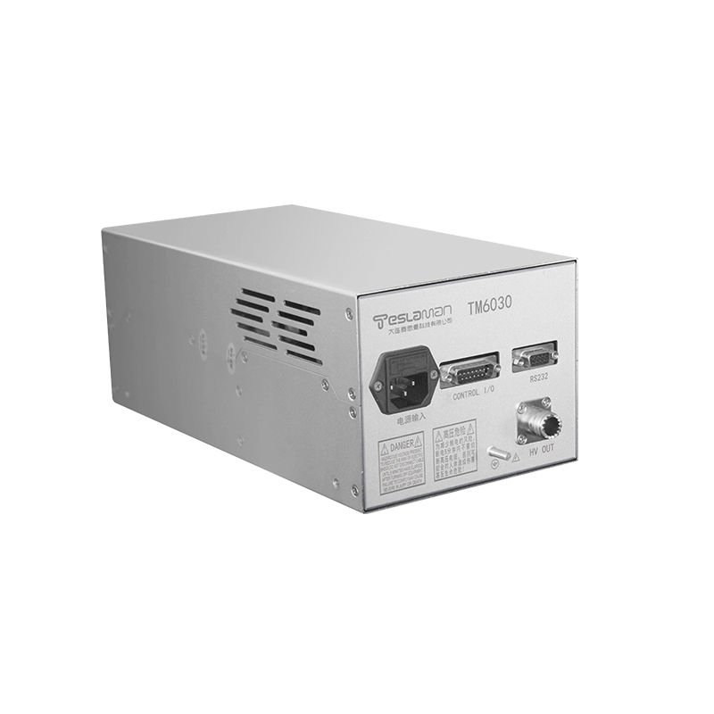
Optimization of Switching Delay of Positive and Negative Switching High-Voltage Power Supply
In numerous electronic devices and scientific research experiments, the positive and negative switching high-voltage power supply plays a crucial role. It can rapidly switch between positive and negative voltages, providing flexible power supply requirements for the system. However, the existence of switching delay often affects the performance of the power supply and the overall stability of the system. Therefore, optimizing the switching delay of the positive and negative switching high-voltage power supply is of great significance.
In terms of principle, the switching delay of the positive and negative switching high-voltage power supply mainly stems from factors such as the response time of the switching elements in the circuit, the charging and discharging processes of energy storage elements like capacitors and inductors, and the processing speed of the control circuit. The switching elements require a certain amount of time to complete the state transition during the on and off moments, which inevitably generates a delay. At the same time, the charging and discharging speed of the energy storage elements also limits the rapid change of the voltage, and if the control circuit cannot issue the switching command in a timely and accurate manner, it will also lead to an increase in the delay.
To optimize the switching delay, we can first start with the selection of switching elements. Selecting high-speed and low on-resistance switching elements can significantly reduce the delay during the switching process. In addition, reasonably designing the switch drive circuit and increasing the rising and falling speed of the drive signal can also accelerate the response speed of the switching elements.
Secondly, the optimized design of the energy storage elements is also crucial. By selecting appropriate capacitance and inductance parameters and reducing their charging and discharging time constants, the speed of voltage change can be accelerated. For example, using capacitors with a low equivalent series resistance (ESR) and inductors with high magnetic permeability can effectively reduce the impact of energy storage elements on the switching speed.
Furthermore, the optimization of the control circuit is the key to reducing the switching delay. Adopting high-performance microcontrollers or digital signal processors (DSPs) and improving the execution speed and accuracy of the control algorithm can achieve faster and more accurate switching control. At the same time, optimizing the control strategy, such as using advanced control methods like predictive control or adaptive control, can predict the voltage change in advance and issue the switching command in advance, thereby reducing the delay.
In addition, a reasonable circuit layout and wiring can also have an impact on the switching delay. Reducing the parasitic capacitance and inductance in the signal transmission path and shortening the transmission distance of key signals can reduce the signal transmission delay and improve the overall response speed of the system.
In conclusion, through the optimization of switching elements, energy storage elements, control circuits, and circuit layouts, the switching delay of the positive and negative switching high-voltage power supply can be effectively reduced, the performance of the power supply and the stability of the system can be improved, and the requirements for the rapid switching of high-voltage power supplies in different application scenarios can be met.