Research on EMI Suppression Technology for High-Voltage Power Supplies in Lithography Machines
Introduction
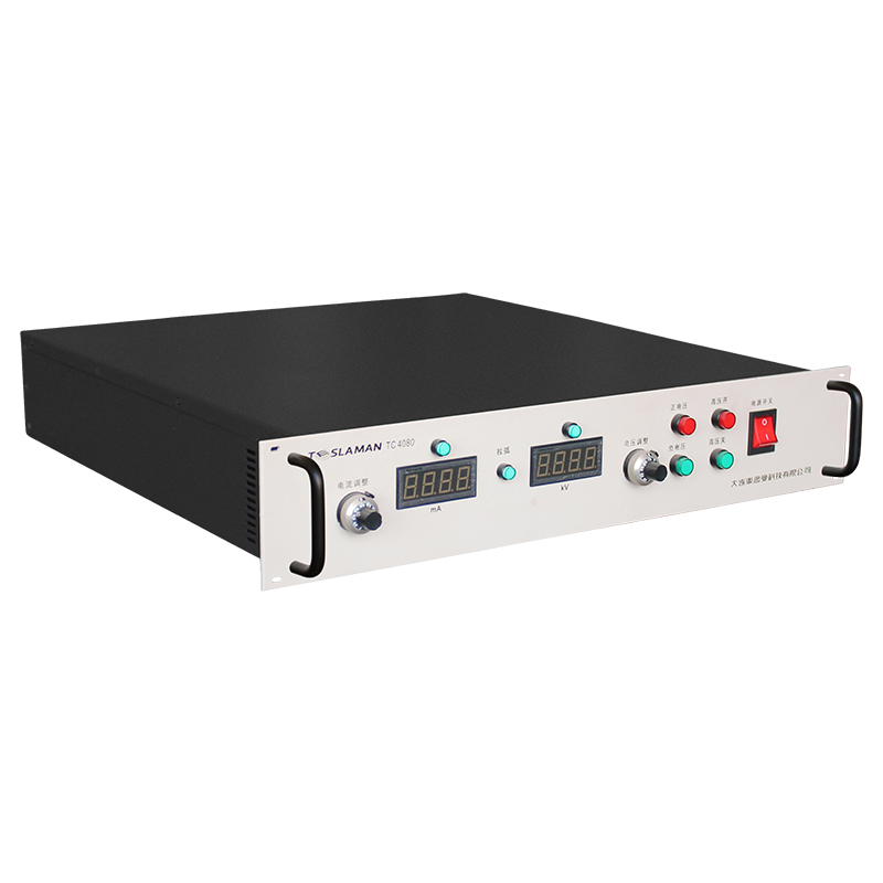
The high-voltage power supply (typically requiring kilovolt-level outputs and milliamp-level currents) in lithography machines is critical for exposure accuracy. However, electromagnetic interference (EMI) generated during switching can couple into precision control systems, causing wafer alignment errors or line-width distortion, making EMI suppression a core challenge in power supply design.
EMI Impact on Lithography Systems
Sensitivity to Conducted Interference
Motion control systems (e.g., wafer and reticle stages) rely on micro-current signals (nanoamp-level). Common-mode interference (coupled via parasitic capacitance to ground) and differential-mode interference (conducted through power lines) can overwhelm control signals, leading to positioning drift.
Radiated Interference and Precision Circuits
High dv/dt (up to 10 kV/μs) during MOSFET turn-off generates broadband radiation (30 MHz–1 GHz), disrupting optical sensors and feedback circuits, and reducing exposure uniformity.
Core Suppression Technologies and Innovations
Resonant Topologies and Soft-Switching
Quasi-Resonant Technology: Switches transistors at voltage valleys (zero-voltage switching), reducing switching losses and EMI by 90%. Ideal for pre-regulation modules.
LLC Series Resonance: Confines switching energy within a narrow band (e.g., 1–2 MHz) using resonant tanks (inductor-capacitor-inductor), minimizing harmonic spread.
Passive Compensation and Magnetic Design
Transformer Parasitic Capacitance Compensation: A compensation winding (1:1 turns ratio) generates counter-phase currents to cancel common-mode noise, reducing it by 12–18 dB.
Magnetic Integration: Combines common-mode chokes and transformers to cancel leakage inductance, shrinking radiation loops by 40%.
Modulated Frequency Control
Spread-Spectrum Clocking (SSCG) modulates fixed switching frequencies (e.g., 100 kHz) into triangular sweeps (±10% offset), dispersing EMI energy over 80–120 kHz and lowering peak EMI by 8–12 dB. Suitable for digital control modules.
Multi-Stage Filtering and Shielding
Three-Stage EMI Filter:
Stage 1: Manganese-zinc core chokes (1–2 mH) for low-frequency noise;
Stage 2: Y-capacitors (2.2 nF) shunt common-mode noise to ground;
Stage 3: Ferrite beads absorb residual high-frequency noise (>100 MHz).
Layered Shielding: Internal copper foil wraps switches/transformers; external permalloy enclosures (permeability >10,000) provide 30 dB radiation attenuation.
Layout and Grounding Optimization
Minimized Loop Layout
Confining high-voltage switches, diodes, and snubbers (RC/RCD) within compact modules (<5 mm trace length) reduces loop inductance radiation.
Split Grounding
Power ground (switches/transformers) and signal ground (control ICs) connect at a single point to prevent contamination;
Low-inductance power planes (<0.5 nH) directly linked to IC pads minimize transient voltage drops.
Conclusion
EMI suppression in lithography power supplies requires integrated approaches: topology optimization (resonant soft-switching), passive compensation (transformer design), frequency modulation, and 3D shielding. Future trends include:
Integrated EMI Filters: Embedding passive components into PCB layers to reduce parasitics;
Adaptive Modulation Algorithms: Dynamically adjusting switching frequencies to avoid sensitive bands.
These techniques can suppress EMI to microvolt levels, meeting the stringent electromagnetic requirements of advanced lithography.