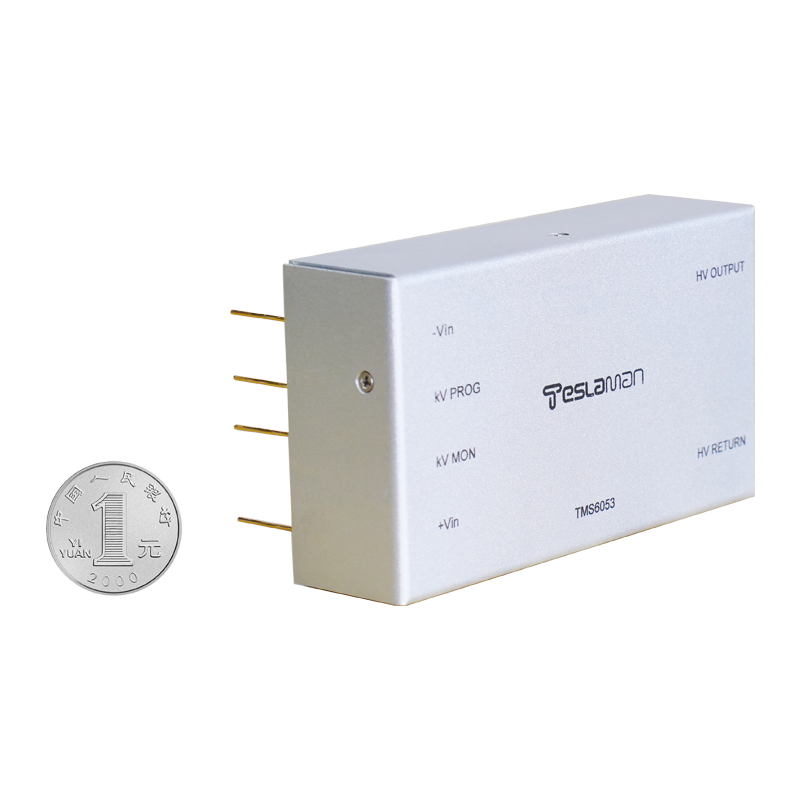
Dynamic Voltage Compensation System for High-Voltage Power Supplies in Ion Implantation: Technology and Applications
In semiconductor manufacturing, ion implantation equipment is a core tool for defining the electrical properties of chips. Its high-voltage power supply (typically outputting –40 kV at 400 W) requires extremely high stability. However, grid voltage sags (instantaneous voltage drops to 10%–90% of nominal values) can cause ion beam fluctuations, leading to deviations in wafer doping concentration and even complete batch scrapping. Statistics show that a single voltage sag event in the semiconductor industry can result in losses of 574,000–3,585,000, far exceeding other industrial sectors. Consequently, Dynamic Voltage Compensation Systems (DVCS) have become a critical solution for ensuring stable operation of high-voltage power supplies in ion implantation.
1. Stringent Voltage Stability Requirements for Ion Implantation
High-voltage power supplies for ion implanters must accelerate ions to MeV energy levels, with output ripple below 0.1% and temperature coefficients ≤25 ppm/℃. If grid voltage sags persist for over 10 ms (e.g., dropping to 70% of rated value):
• Beam Current Instability: Electric field fluctuations cause ion beam deviation, degrading doping uniformity.
• Equipment Protection Shutdown: Precision control systems (e.g., PLCs) trigger interrupt programs when voltage drops to 30%–70%.
• Auxiliary System Failure: Vacuum pumps and cooling water units shut down, indirectly halting the implantation process.
2. Core Technical Solutions of DVCS
Modern DVCS employs a multi-level cooperative control architecture:
1. Core Architecture
• Supercapacitor Energy Storage: Replaces traditional batteries, offering millisecond response (<2 ms) and high cycle life (>1 million cycles), pre-charged via a rectifier module.
• Cascaded H-Bridge Inverter: Multiple single-phase full-bridge submodules connected in series to output –40 kV. Each submodule includes four IGBT switches and a DC capacitor, with voltage scalability achieved through positive/negative cascading.
• Fully Controlled Static Switch: Comprising anti-parallel diodes and IGBTs, with turn-off time <100 μs—50 times faster than thyristor solutions—enabling microsecond isolation between grid and load.
2. Control Strategies
• Voltage-Current Dual-Loop Control: Real-time monitoring of load voltage U_L and grid voltage U calculates compensation voltage amplitude \Delta U = \sqrt{U_{ref}^2 U^2} and phase \(\theta = \arccos(U/U_{ref})\) to ensure synchronization.
• dq Feedforward Decoupling Control: Decomposes parameters like filter capacitor voltage and inductor current into active/reactive components, suppressing coupling interference via feedforward compensation to enhance dynamic response accuracy.
• Capacitor Voltage Balancing Control: Addresses DC-side voltage imbalance in cascaded H-bridges by generating target switching signals to regulate submodule charge/discharge states, preventing system oscillation.
3. Modular Coordination Mechanism
Multiple DVCS modules operate in parallel via a fiber-optic loop network. When the main control unit detects grid abnormalities, optical signals trigger synchronous shutdown of all static switches, enabling millisecond-level coordinated switching and scalable compensation capacity.
3. Application Value and Technical Prospects
DVCS delivers significant benefits for ion implantation:
• Economic Impact: Compliance with SEMI F47 standard (tolerating 50% voltage sag for 10 cycles) reduces wafer scrap rates by >90%.
• Energy Efficiency: System efficiency >98%, with energy storage modules dormant during standby and inverters activated only during compensation, consuming <1/3 the power of traditional UPS.
• Technical Scalability: Integrates with power quality monitoring systems (e.g., IEEE 1159-2019) to predict sag events and initiate preventive compensation.
Conclusion
The DVCS for ion implantation high-voltage power supplies combines a supercapacitor + cascaded H-bridge + fully controlled switch architecture with multi-module fiber-optic coordination and dual-loop control to achieve microsecond-level voltage sag compensation. This solution not only meets extreme power quality requirements but also standardizes voltage protection for semiconductor manufacturing through modular design. With the adoption of wide-bandgap semiconductor devices (e.g., SiC IGBTs), DVCS will further improve in response speed and power density, becoming critical infrastructure for advanced-node chip manufacturing.