Intelligent Process Window Optimization for High-Voltage Power Supply in Etching Equipment
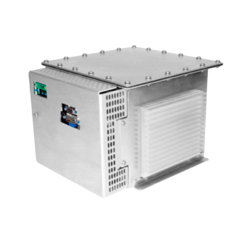
Etching process is a key link in "pattern transfer" in semiconductor manufacturing. It requires high-voltage power supplies to drive plasma (e.g., CF4, O2 plasma) for selective etching of wafer surface materials. The width of the process window (i.e., the parameter range meeting indicators such as "etching rate ≥ 500 nm/min, etching selectivity ≥ 20:1, uniformity ≤ 3%") directly determines the etching yield. Traditional process window debugging relies on engineers' experience-based trial and error: by adjusting parameters of the high-voltage power supply one by one, such as output voltage (1-5 kV), pulse frequency (10-100 kHz), and duty cycle (20%-80%), each debugging consumes 20-30 test wafers and takes 2-3 days. Moreover, it is difficult to adapt to the differentiated needs of multi-variety wafers (e.g., logic chips, memory chips). When the wafer material or etching pattern changes, the trial-and-error process needs to be restarted, resulting in low production efficiency.
The intelligent process window optimization technology significantly shortens the optimization cycle and improves parameter accuracy based on a digital approach of "data modeling - algorithm optimization - real-time feedback." In the data modeling stage, this technology builds a process prediction model through "small-sample + transfer learning": first, collecting 10-15 groups of corresponding data between basic parameters (voltage, frequency, duty cycle) and etching effects (rate, selectivity, uniformity), using the random forest algorithm to establish a preliminary model, then fusing historical data of similar etching processes (e.g., etching rules of different wafer materials) through transfer learning, improving the model prediction accuracy to over 95% and avoiding consumption of a large number of test wafers. In the algorithm optimization stage, an improved particle swarm optimization algorithm is adopted, converting etching rate, selectivity, and uniformity into a multi-objective optimization function, and finding the "optimal parameter combination" through particle iterative search (number of iterations ≤ 50). For example, for deep trench etching of 3D NAND memory chips, the algorithm can determine parameters of "voltage 3.2 kV + frequency 45 kHz + duty cycle 55%" within 30 minutes, achieving an etching rate of 620 nm/min, selectivity of 25:1, and uniformity of 2.1%. In the real-time feedback stage, an online plasma diagnostic system (e.g., Langmuir probe) monitors the etching process. When the etching effect deviates due to wafer batch changes, the power supply can automatically correct parameters (e.g., increasing voltage by 0.1 kV when the etching rate decreases by 5%), ensuring process stability.
The practical application of this technology has achieved remarkable results: after adopting this technology, a semiconductor factory shortened the etching process debugging time from 3 days to 2 hours, reduced test wafer consumption by 80%, and improved the switching efficiency of multi-variety wafers by 3 times. Meanwhile, intelligent optimization increased the etching yield from 88% to 96%, reducing waste costs by over one million yuan annually. With the development of semiconductors towards "heterogeneous integration" and "3D stacking," this technology will further integrate digital twin technology, building a full-process system of "virtual etching - real optimization," and providing more flexible power parameter solutions for the etching of complex-structured wafers.