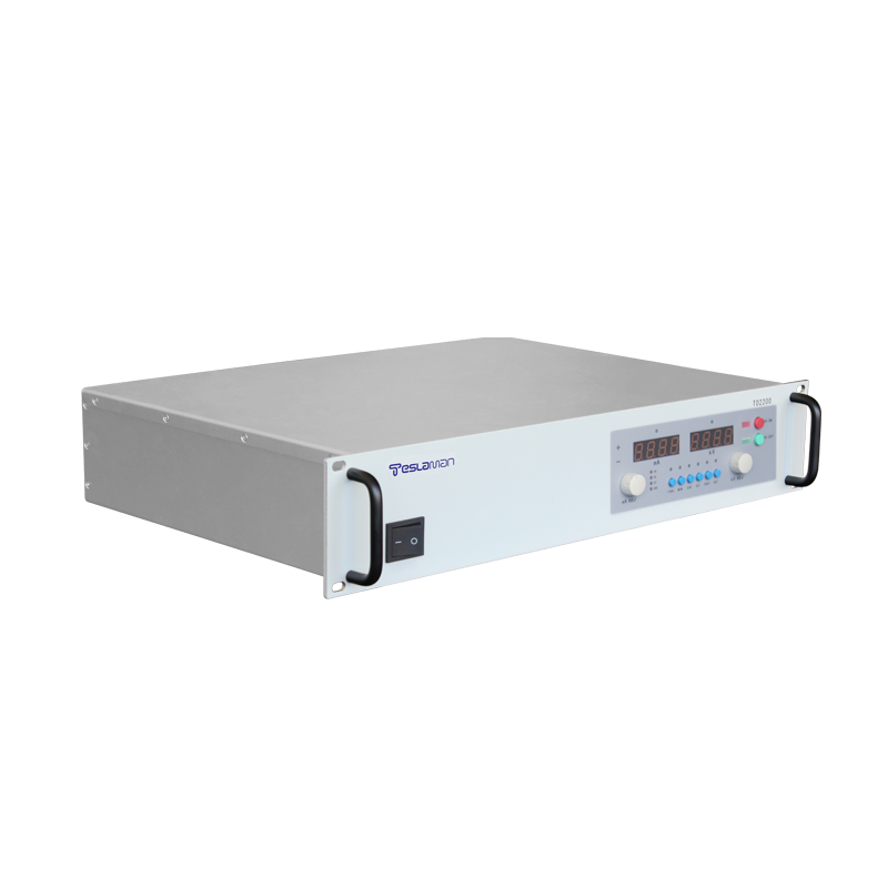
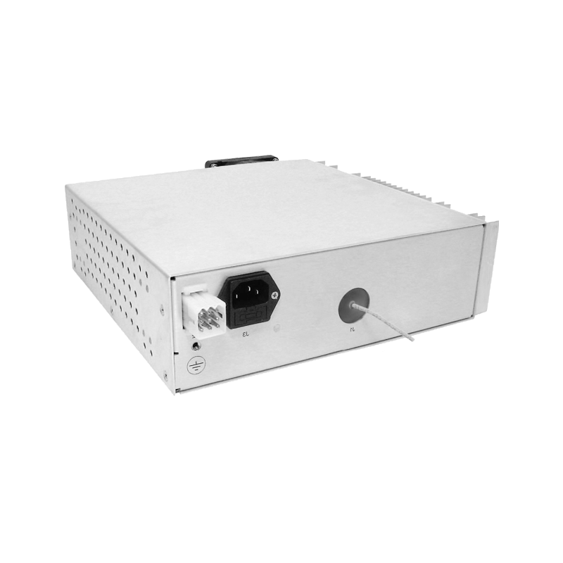
Electrostatic Chuck Multi-Frequency Drive High-Voltage Power Supply
The evolution of plasma processing in semiconductor manufacturing, particularly in advanced etching and deposition, has introduced stringent requirements for substrate temperature control and RF coupling efficiency. The electrostatic chuck (ESC), responsible for clamping the wafer, is no longer a simple DC-biased electrode. Modern processes, especially those utilizing very high-frequency (VHF) or multiple RF biases, demand ESCs that can operate with multi-frequency high-voltage drives. This specialized power supply applies a composite high-voltage waveform to the chuck electrodes, typically consisting of a DC component for clamping force and one or more AC components for enhanced thermal control or plasma coupling, fundamentally altering the chuck's functionality from a passive holder to an active process component.
The primary driver for multi-frequency operation is the management of the thermal interface between the wafer and the chuck. In high-power processes, the wafer temperature must be precisely regulated. The traditional method uses a backside helium gas for heat transfer, but its efficacy is limited by the microscopic roughness of the surfaces. A multi-frequency ESC supply addresses this by generating an AC electric field in addition to the DC clamping field. This AC field, often in the kHz to low MHz range, induces motion in polar molecules (like water vapor) or charged particles trapped in the interface, effectively "stirring" the interfacial gas and dramatically improving its thermal conductivity. This is known as the electro-thermal or "Johnsen-Rahbek" effect enhancement via AC bias. The supply must generate this AC high voltage (typically several hundred volts peak-to-peak) superimposed on the kilovolt-level DC bias, with precise control over the AC frequency and amplitude, as these parameters directly influence the thermal conductance and must be tuned for different process conditions.
A more advanced application involves using the ESC as a secondary electrode for plasma control. In dual-frequency capacitively coupled plasma etchers, one RF (e.g., 60 MHz) controls plasma density, while a lower-frequency RF (e.g., 2 MHz) controls ion bombardment energy on the wafer. By applying a portion of this lower-frequency RF bias directly to the ESC electrodes through a multi-frequency supply, the system can achieve more independent control over ion energy and flux at the wafer surface, improving process uniformity and feature profile control. Here, the supply must deliver high-voltage RF power (tens to hundreds of volts RMS) at MHz frequencies, synchronized and phase-locked to the main RF generators, while maintaining the DC clamping potential.
The architecture of such a supply is inherently complex. It is a multi-channel system where channels are not independent but must be combined at a high-voltage output node without destructive interference. The DC channel is a high-stability, low-ripple supply capable of sourcing and sinking current, as the wafer potential can fluctuate. The AC or RF channels are linear or switching amplifiers designed for high-voltage, high-frequency operation. They must have low output impedance at their operating frequencies to drive the capacitive load of the ESC (often hundreds of picofarads to nanofarads) without significant phase shift or attenuation. The outputs of these channels are combined via high-voltage, wideband coupling networks. A common method uses a bias tee-like structure: an inductor that passes DC but blocks AC is placed in series with the DC supply, while a capacitor that passes AC but blocks DC is placed in series with the AC supply, with both paths meeting at the output.
Control and stability are monumental challenges. The different frequency components interact through the non-linear plasma load and the chuck's semiconductor dielectric layer. The DSP-based controller must manage real-time impedance matching for the RF channels, adjust the DC level to compensate for plasma-induced DC bias shifts, and prevent any instability such as parasitic oscillations. Furthermore, the timing of the application of these frequencies is critical. During wafer de-clamping, the voltages must be ramped down in a specific sequence to prevent charge trapping that could make wafer removal difficult or cause damage. The system includes extensive diagnostics, monitoring the DC current (which indicates leakage and clamping force) and the AC/RF current and phase for each channel, providing data for closed-loop control and fault detection.
Reliability in the plasma environment is non-negotiable. The entire supply is heavily shielded against the intense RF fields from the process chamber. All signal and control lines are fiber-optic or passed through feedthroughs with high common-mode rejection. The output stage is designed to withstand and quickly recover from arc events, which are common when processing wafers with defects or during chamber conditioning. By integrating multiple high-voltage frequencies into a single, coherent output, this power supply transforms the electrostatic chuck into a multi-functional tool, enabling unprecedented control over wafer temperature, ion energy distribution, and ultimately, the critical dimensions and uniformity of devices at the nanoscale.