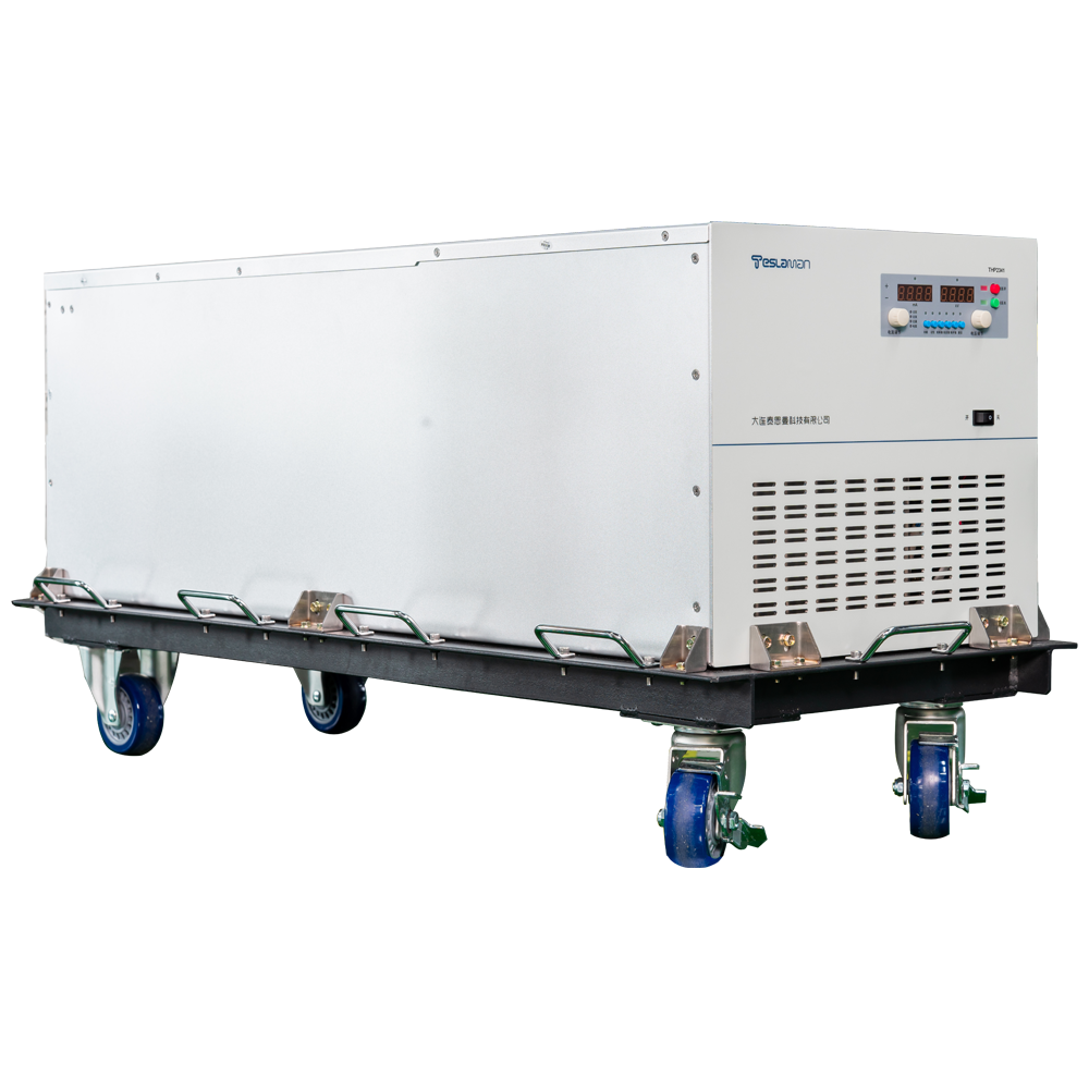
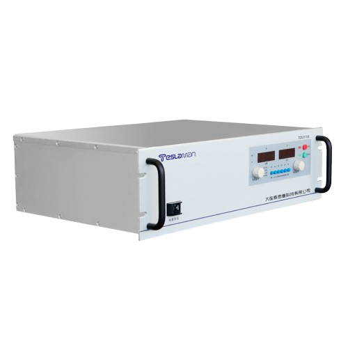
Electrostatic Chuck Double-Side Clamping High-Voltage Balance Power Supply
Modern plasma etch and chemical vapor deposition processes place extraordinary demands on wafer temperature uniformity and thermal management. The electrostatic chuck (ESC), which replaces mechanical clamping, has become the standard for securing wafers, especially for thin and large-diameter substrates. The double-side clamping ESC, which utilizes electrodes on both the chuck surface and a facing electrode, represents a significant evolution. Its operation fundamentally relies on a high-voltage balance power supply, a system engineered to apply and meticulously control complementary high voltages to these two electrodes. This creates a powerful and uniform electrostatic field that grips the wafer from both sides, ensuring intimate thermal contact across the entire backside, a critical factor for process repeatability.
The term 'balance' is the operative principle. The power supply does not simply output two independent high voltages. It dynamically regulates the potential difference between the top and bottom electrodes while maintaining a defined common-mode voltage. This active balancing is crucial for several reasons. Firstly, it maximizes the clamping force uniformly, preventing wafer slippage or micro-vibrations during high-pressure plasma processing. Secondly, and more subtly, it provides exquisite control over the DC bias that develops on the wafer. In RF-driven plasmas, the wafer naturally assumes a negative DC bias relative to the plasma. The balance power supply can influence this self-bias by adjusting the potentials on the dual electrodes, thereby offering a new degree of freedom to control ion bombardment energy independently of other plasma parameters. This is a powerful lever for optimizing etch anisotropy or deposition film quality.
Designing such a power supply involves overcoming substantial technical hurdles. It must deliver two high-voltage outputs, often in the kilovolt range, with precise synchronization and stability. Any imbalance or drift between the outputs can lead to uneven clamping, resulting in localized hot spots or poor heat transfer, which directly translates into non-uniform etch rates or film thickness. The feedback control system must continuously monitor both voltages and the clamping current, making real-time adjustments to maintain the set balance ratio. Furthermore, the system must be designed for the harsh environment of a process chamber. It requires excellent immunity to conducted and radiated RF noise from the plasma, which can easily corrupt sensitive voltage measurement signals. Robust isolation, both between the two high-voltage outputs and from the control system, is mandatory for safety and to prevent ground loops. The emergence of these sophisticated balance power supplies has been instrumental in enabling the transition to 300mm wafers and beyond, where thermal management challenges are exponentially greater.