Adaptive High-Voltage Power Supply for Electrostatic Chucks Accommodating Wafer Warpage
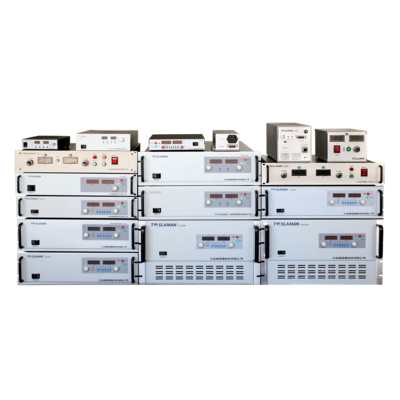
Modern semiconductor fabrication utilizes wafers that are increasingly thin, particularly for memory and advanced packaging applications, making them highly susceptible to warpage from thermal and mechanical stresses. This warpage presents a significant challenge for electrostatic chucks (ESCs), as a non-flat wafer cannot achieve uniform intimate contact with the chuck surface, leading to localized thermal runaway, process non-uniformity, and particle generation. An adaptive high-voltage power supply system is designed to dynamically compensate for this warpage by modulating the clamping field in response to real-time wafer topography, ensuring uniform clamping force across the entire wafer surface.
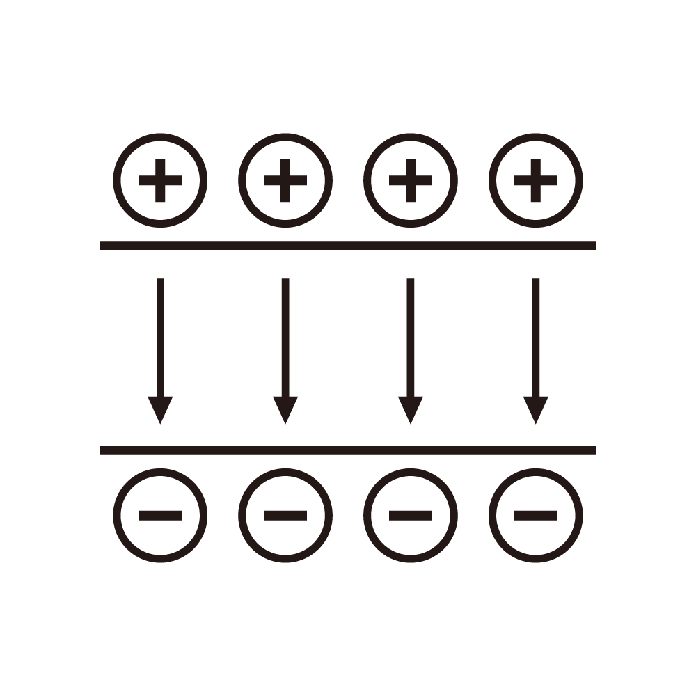
The traditional ESC applies a uniform electric field between its buried electrode and the wafer. If the wafer is warped, areas with poor contact experience a larger air gap. The clamping force is inversely proportional to the square of this gap distance. Therefore, bowed areas experience drastically reduced force, potentially losing clamping altogether. The adaptive system addresses this by segmenting the ESC electrode into multiple independently controllable zones, often arranged in a radial or grid pattern. Each zone is driven by its own high-voltage channel from a multi-output power supply or a single supply with a fast-switching distribution network. The core innovation lies in the feedback mechanism that determines the optimal voltage for each zone.
This feedback is typically provided by a network of capacitive or pressure sensors embedded in the chuck surface. As the wafer is lowered onto the chuck, these sensors map the local gap distance or contact pressure. This topographical data is fed to a control algorithm that calculates the required electric field strength for each zone to achieve a target clamping pressure. The relationship is complex, involving the dielectric properties of the chuck coating and the wafer, and the non-linear force-gap relationship of the electrostatic attraction. The algorithm outputs a set of voltage commands for each zone. Zones under a bowed region (large gap) receive a higher voltage to increase the field strength and compensate for the gap, while zones with good contact receive a standard voltage.
The high-voltage power supply for such a system must possess several key characteristics. First, each output channel must be independently programmable with fine voltage resolution, often on the order of 1 volt, across a range that may span from a few hundred volts to several kilovolts. Second, the channels must be perfectly isolated from each other to prevent cross-talk, as any electrical leakage between zones would defeat the purpose of independent control. This isolation extends to both the DC output and the control signals, typically requiring isolated DC-DC converters and digital isolators. Third, the system must respond quickly. While the initial mapping and voltage setting occur during wafer load, some processes may induce dynamic warpage changes due to heating. The power supply must be capable of adjusting zone voltages on a timescale of seconds to track these changes.
Implementation involves significant integration with the wafer handling system. The mapping sequence must be fast to maintain throughput. Often, a coarse map is generated as the wafer descends, followed by a fine-tuning phase after initial contact. The safety implications are also critical. Applying different potentials to adjacent electrodes on the chuck increases the risk of inter-electrode breakdown, especially in the presence of plasma. Therefore, the dielectric strength and creepage distance between electrode zones in the chuck design are paramount, and the power supply must include individual arc detection for each channel. Furthermore, the system must gracefully handle edge effects and partial wafer coverage, adjusting the outer zone logic accordingly.
Beyond merely clamping a warped wafer, this technology enables process benefits. By ensuring uniform thermal contact, it eliminates hot spots that can cause within-wafer critical dimension variation in etch or deposition steps. It also allows for the safe processing of intentionally warped wafers, such as those used in wafer-level packaging after through-silicon via (TSV) formation. The adaptive high-voltage supply thus transforms the ESC from a passive clamping device into an active shape-conforming system, expanding the process window and improving yield for the most challenging thin-wafer applications.
