Monitoring Wafer Backside Contamination on Electrostatic Chucks Through High Voltage Leakage Analysis
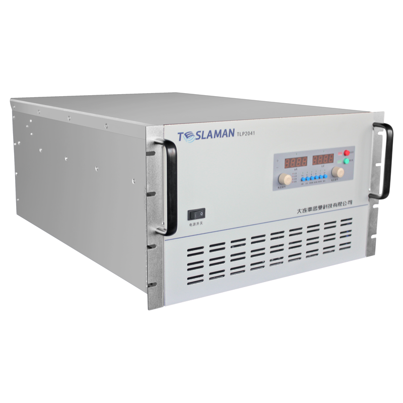
The electrostatic chuck has become an indispensable component in modern semiconductor processing, providing the means to securely hold a wafer in place without mechanical clamping, which can cause particle generation. In plasma etch and deposition systems, the ESC utilizes a powerful high voltage to induce an electrostatic force between the chuck and the wafer. While the primary function of this high voltage is to provide a strong, uniform clamping force, often in conjunction with a backside helium cooling flow, the electrical behavior of the chuck-wafer interface offers a wealth of information for process control. Specifically, the monitoring of the backside of the wafer for contamination has emerged as a critical application of high voltage systems. The principle is elegantly simple yet deeply rooted in the physics of leakage currents. A standard ESC operates by applying a high DC voltage, often in the kilovolt range, to electrodes embedded within the ceramic chuck body. The wafer, which is typically either grounded or allowed to float electrically, is attracted to the chuck surface. The interface between the wafer backside and the chuck surface is not perfect; it is a region of microscopic contact points and gaps. This interface is deliberately filled with helium gas to facilitate thermal transfer. However, if the backside of the wafer becomes contaminated, for example, with a thin film from a previous process step, a metallic flake, or a residual chemical, the electrical properties of this interface change dramatically. A conductive contaminant can provide a leakage path from the wafer, through the helium gap, to ground or to other chuck electrodes. This leakage current can be detected and analyzed by the high voltage power supply itself. In sophisticated process tools, the power supply is not just a static voltage source; it is an active monitoring device. By precisely measuring the current required to maintain the clamping voltage, or by performing a controlled high voltage ramp test, the system can infer the condition of the wafer backside. A sudden increase in leakage current, for instance, might indicate that a wafer has a backside metal film that was not completely removed in a prior clean step. This is not merely a theoretical concern; I have seen instances where such contamination leads to catastrophic arcing, damaging both the wafer and the expensive ESC. The high voltage, in this monitoring role, becomes a sensor. The power supply must be capable of resolving microampere or even nanoampere level changes in leakage current against a background of the much larger capacitive charging currents and the normal operational currents. This requires a power supply with exceptional sensitivity and dynamic range. Furthermore, the interpretation of this data is key. A seasoned process engineer learns to distinguish between a leakage current caused by a backside particle, which might be localized and cause a sharp, intermittent current spike, and a broad, diffuse contamination, which might cause a steady, uniform increase in leakage. The high voltage system thus serves as a silent guardian, providing an in-situ, real-time monitor of a critical aspect of wafer condition that is otherwise invisible. This proactive monitoring prevents yield loss and tool downtime, proving that the application of high voltage extends far beyond its brute-force function of mechanical clamping.