Real-Time High-Voltage Compensation for Wafer Warpage in Electrostatic Chucks
The electrostatic chuck has become an indispensable tool in semiconductor manufacturing, particularly for processes like etching and deposition that require precise temperature control and rigid wafer clamping in a vacuum environment. The principle is elegantly simple: a high voltage, typically several hundred to a few thousand volts, is applied to electrodes embedded within a ceramic body. This generates an electrostatic force that pulls the wafer flat against the chuck surface, ensuring excellent thermal contact and preventing movement. However, the modern semiconductor process is anything but simple. Wafers are subjected to extreme thermal budgets and thin-film stresses that can cause them to warp, bow, or twist. This wafer warpage presents a fundamental challenge to the electrostatic chuck. If the chuck cannot conform to the warped shape, or if it applies a non-uniform clamping force, localized gaps can form, leading to hotspots, process non-uniformity, and even wafer breakage. In my five decades of working with high-voltage systems in semiconductor equipment, I have witnessed the evolution of the electrostatic chuck from a simple on-off clamping device to a sophisticated, actively controlled system where the high-voltage supply plays a central role in real-time warpage compensation. This is no longer just about holding the wafer; it is about dynamically shaping the electrostatic field to flatten it.
The physics of electrostatic clamping is governed by the Johnsen-Rahbek effect for semiconductors and the Coulombic force for insulators. When a voltage is applied, an electrostatic pressure develops between the wafer and the chuck, inversely proportional to the square of the gap distance. A uniform gap results in a uniform clamping force. However, a warped wafer will have a variable gap across its surface. In regions where the wafer bows away from the chuck, the gap is large, and the clamping force is weak. In regions where it touches or is very close, the force is strong. This non-uniform pressure can itself exacerbate the warpage, creating a feedback loop that may lead to loss of control. The first line of defense against this is a stiff, flat chuck surface, but with extreme wafer warpage becoming more common, this is no longer sufficient. The solution lies in the electrode design. A modern electrostatic chuck is not a single electrode but a complex array of individually addressable zones, often arranged in concentric rings or a grid pattern. By applying different voltages to these different zones, we can tailor the clamping force profile to match the wafers shape. If the center of the wafer is bowed upward, we can apply a higher voltage to the central electrode zone to pull it down more forcefully. If the edge is lifting, we can increase the voltage at the edge zones. This is the essence of real-time compensation.
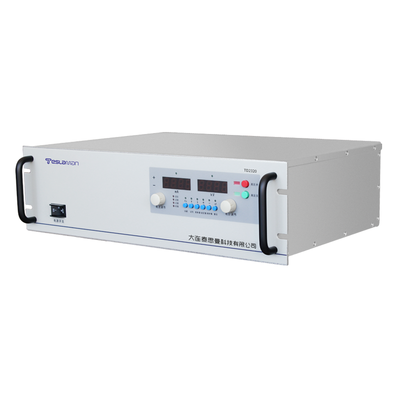
The implementation of this zoned clamping requires a multi-channel high-voltage power supply of considerable sophistication. Each zone requires its own independently programmable high-voltage output, capable of being adjusted from zero up to several kilovolts with high resolution and stability. The power supplies must be able to source the current required to charge the capacitance of the chuck and the wafer, but more importantly, they must be able to sink current as well, to rapidly reduce the voltage on a zone if the control algorithm calls for it. This is a demanding requirement, as the chuck is a highly capacitive load. The switching or amplification stages for each channel must be carefully designed to avoid cross-talk between zones, as a change in voltage on one electrode can capacitively couple to its neighbors, disturbing the carefully calculated field pattern. The control system for such a chuck is a marvel of real-time engineering. It must take input from sensors that measure the wafer shape. These sensors can be optical, measuring the gap through the chuck, or they can be based on capacitance or even on the backside gas pressure used for heat transfer. This data is fed into a model that calculates the ideal voltage for each zone to achieve a flat wafer. The high-voltage supplies must then respond to these commands with a speed that matches the thermal or mechanical time constants of the system, which could be milliseconds to seconds. The result is a closed-loop, active flattening system that can compensate for warpage that would otherwise render a wafer unprocessable. In my long career, I have seen many technological leaps, but the development of actively compensated electrostatic chucks stands out as a prime example of how high-voltage engineering, when combined with advanced sensing and control, can solve seemingly intractable problems in manufacturing, enabling the continued scaling of semiconductor devices on increasingly fragile and stressed substrates.