Synergistic High-Voltage Annealing for Ultra-Shallow Junction Formation in Ion Implantation
The relentless scaling of semiconductor devices has demanded ever-shallower and more highly doped source and drain regions, known as ultra-shallow junctions. Ion implantation is the primary method for introducing dopant atoms into silicon, but it comes with a significant penalty: lattice damage. As high-energy ions crash into the crystal, they displace silicon atoms, creating a cascade of defects and leaving the implanted region amorphous. To repair this damage and to electrically activate the dopants, meaning to move them into substitutional lattice sites where they can contribute charge carriers, a high-temperature annealing step is required. For decades, rapid thermal annealing, using banks of intense lamps, has been the workhorse for this process. However, as junction depths have shrunk to below 10 nanometers, the thermal budget of even the fastest lamp-based anneals has become a limiting factor. The need to activate dopants without allowing them to diffuse deeper into the substrate has driven the exploration of alternative annealing techniques. One of the most promising, and one that I have followed closely in my career, is the use of high-voltage electric fields in synergy with thermal energy to achieve activation at significantly lower temperatures. This is known as high-voltage or field-assisted annealing.
The fundamental problem with conventional annealing is that the diffusivity of dopants in silicon is strongly temperature-dependent. To achieve high activation, we need to heat the wafer to temperatures where the dopants become highly mobile, which inevitably causes them to diffuse, broadening the junction. The goal of low-temperature annealing is to provide the energy needed for defect repair and dopant incorporation without providing enough energy for significant diffusion. This is where an applied electric field can play a transformative role. When a high voltage is applied across a silicon wafer during annealing, it creates an electric field within the material. This field can exert a force on charged point defects, such as vacancies and interstitials, and on the dopant ions themselves. This force can enhance the kinetics of defect recombination and can actively drive dopants into substitutional sites. The effect is akin to biasing the random walk of atoms, steering them toward configurations that are electrically active.
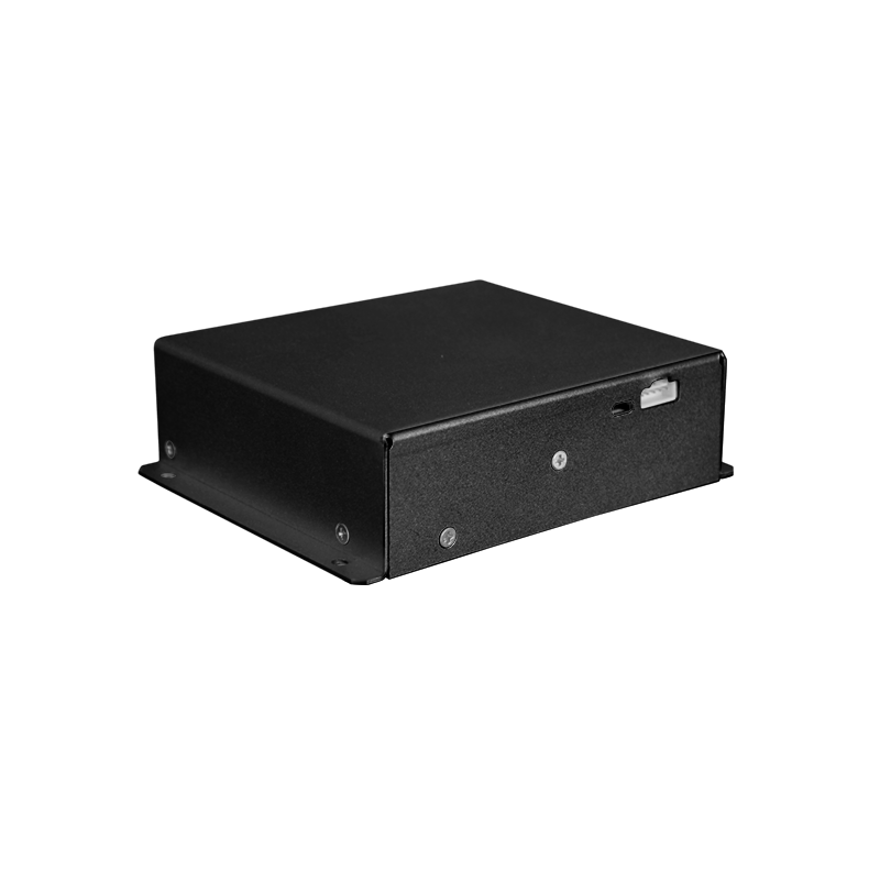
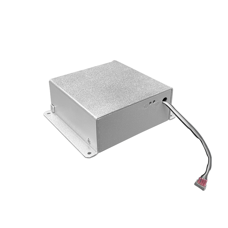
The implementation of high-voltage annealing requires a specialized apparatus. The wafer must be held between two electrodes that can withstand the annealing temperature, which can still be several hundred degrees Celsius. A high-voltage power supply, capable of delivering a stable, programmable voltage of perhaps several kilovolts, is connected to these electrodes. The supply must be able to operate in a vacuum or a controlled atmosphere, and it must be carefully isolated from the heating elements and the chamber walls to prevent leakage currents. The polarity of the applied voltage can be chosen to enhance the desired effect. For example, a positive bias on the front side of the wafer might attract negatively charged dopant-vacancy complexes, facilitating their dissociation and the subsequent incorporation of the dopant. The current flowing through the wafer during the anneal is typically very small, as the silicon is not highly conductive at these temperatures, but it must still be monitored as it provides insights into the kinetics of the process.
The synergy between the thermal and electrical stimuli is the key. The elevated temperature provides the base energy for atomic motion, while the electric field provides a directional bias. By carefully optimizing the temperature and the voltage, we can achieve a level of dopant activation that would otherwise require a much higher temperature. This has been demonstrated in research for various dopants, including boron and phosphorus. The technique also offers the potential for selective activation. By using a patterned electrode on the front side of the wafer, we could apply the field only to specific regions, activating dopants in the source and drain areas while leaving other regions unaffected. This would eliminate the need for some of the masking steps in the conventional flow. In my long career, I have seen many proposed alternatives to conventional annealing come and go. High-voltage annealing, however, stands out because it directly addresses the fundamental physics of the problem. It adds a new control knob, the electric field, to the process engineer s toolkit. The challenge now lies in developing the high-voltage hardware and the process models necessary to bring this promising technique from the research lab into high-volume manufacturing. If successful, it could be a key enabler for the next several generations of semiconductor technology, allowing us to create the ultra-shallow junctions that are the bedrock of modern electronics, without the thermal penalty that has long constrained us.