High-Voltage Modulation for Sidewall Passivation in Reactive Ion Etching
Reactive ion etching has been, for decades, the workhorse of microfabrication, enabling the transfer of intricate patterns into silicon, dielectrics, and metals with high fidelity. As device dimensions have shrunk into the nanometer regime, the demands on the etching process have become increasingly stringent. One of the most critical challenges is achieving anisotropic etching, where material is removed vertically with minimal undercutting of the masking layer. This is particularly difficult when etching deep, high-aspect-ratio features. The solution to this challenge lies in a delicate balance between etching and deposition, a balance that is often controlled by the application of a high-voltage bias to the substrate. In my years of research at the intersection of plasma physics and microfabrication, I have seen the evolution of this technique, where the modulation of the substrate bias voltage is used to control the deposition of passivation layers on the feature sidewalls.
The fundamental physics of reactive ion etching involves generating a plasma containing both chemically reactive species, such as fluorine or chlorine radicals, and energetic ions. The substrate to be etched is placed on a electrode that is powered by a radio-frequency source, creating a negative DC self-bias. This bias accelerates positive ions from the plasma vertically towards the substrate. These energetic ions bombard the horizontal surfaces, enhancing the chemical etching reactions and providing the directionality needed for anisotropic profiles. However, the ions also bombard the sidewalls of features if they have any angular spread, leading to unwanted lateral etching or bowing.
To prevent this lateral etching, a passivation layer is deposited on the feature sidewalls. This layer, typically a fluorocarbon polymer or a silicon oxide-like material, is resistant to the chemical etchant. It protects the sidewall while the horizontal surfaces at the bottom of the feature continue to be etched by the combined action of ions and reactive neutrals. The classic example is the Bosch process for deep silicon etching, which alternates between an etching step using sulfur hexafluoride and a deposition step using a fluorocarbon gas like octafluorocyclobutane. However, for many critical etching steps, this time-multiplexed approach can introduce scalloping on the sidewalls. An alternative and more elegant method is to perform the etching and deposition simultaneously, and to control the balance between them through the high-voltage bias applied to the substrate.
In a simultaneous etch/deposition process, the plasma contains both the etchant and the deposition precursor gases. The deposition of the passivation layer occurs on all surfaces, but it is preferentially removed from horizontal surfaces by ion bombardment. The key parameter is the energy of the ions, which is controlled by the substrate bias voltage. If the bias voltage is high, the ions have enough energy to sputter away the passivation layer from the bottom of the feature, allowing the etch to proceed. If the bias voltage is low, the passivation layer remains intact, and net deposition occurs. By carefully selecting the bias voltage, one can achieve a regime where the passivation layer is removed from the bottom but remains on the sidewalls, enabling a highly anisotropic etch.
This is where the concept of high-voltage modulation becomes critical. In advanced etching processes, a constant bias voltage is often insufficient to achieve the desired profile over the entire depth of a high-aspect-ratio feature. As the feature deepens, the transport of ions and neutrals to the bottom becomes more difficult. The flux of ions to the bottom decreases, while the flux of deposition precursors may also be affected. To compensate for these transport effects, the bias voltage may need to be modulated as a function of time or as a function of feature depth. For example, at the beginning of the etch, when the feature is shallow, a moderate bias may be sufficient. As the feature deepens, the bias may need to be gradually increased to maintain a sufficient ion energy at the bottom to clear the passivation layer. This is often referred to as voltage ramping or voltage profiling.
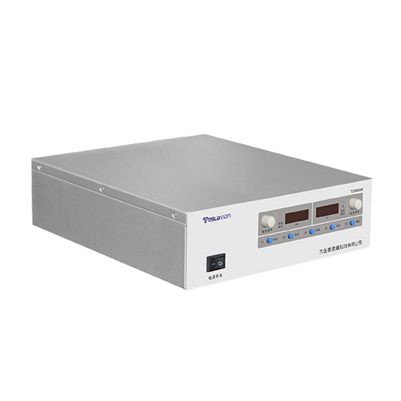
The power supply that provides this substrate bias must therefore be capable of more than just delivering a stable RF voltage. It must be capable of precise, dynamic modulation. In an RF system, the DC self-bias is a function of the RF voltage amplitude, the plasma impedance, and the electrode geometry. To achieve a desired bias voltage profile, the RF power supply must be controlled by a sophisticated waveform generator and feedback system. The supply must be able to ramp its output power smoothly and linearly, or to step it to a new value, all while maintaining a stable plasma and a clean RF waveform. Any instability or noise in the bias voltage will be directly translated into variations in the ion bombardment energy, leading to microloading effects, aspect-ratio-dependent etching, or profile anomalies like notching or bowing.
In my research group, we have explored the use of pulsed bias voltages to gain even greater control. By pulsing the bias on and off at kilohertz or megahertz frequencies, we can create a time-averaged ion energy distribution that is a blend of high-energy and low-energy components. The high-energy component during the pulse-on time clears the passivation from the bottom, while the low-energy or zero-energy component during the pulse-off time allows for a more isotropic deposition on the sidewalls or for the neutralization of charging effects. The duty cycle and frequency of the bias pulses become additional tuning knobs for the process engineer. This pulsed biasing requires an RF power supply with an exceptionally fast response time, capable of turning on and off within microseconds and of synchronizing with other pulsed sources in the plasma chamber.
The interaction between the bias power supply and the main plasma source power supply adds another layer of complexity. In many etching systems, the plasma is sustained by an inductively coupled source operating at one frequency, while the bias is applied at another frequency. The two power supplies can interact through the plasma, leading to cross-coupling and instability. Advanced etching systems now incorporate sophisticated synchronization and control schemes, where the phase and timing of the two supplies can be adjusted to minimize this interaction. The high-voltage bias supply, once a simple accessory, has become a central and dynamic element in the precise sculpting of materials at the nanometer scale, enabling the continued miniaturization of the devices that power our modern world.