Power Pulse Shaping Technology of High Voltage RF Bias Power Supply in Atomic Layer Precision Etching
Atomic layer etching represents the ultimate precision in semiconductor manufacturing, enabling removal of material one atomic layer at a time. This level of precision requires extraordinary control over the plasma conditions and ion energies that accomplish the etching. The high voltage radio frequency bias power supply plays a central role in controlling the ion bombardment energy, and pulse shaping technology enables the fine control necessary for atomic layer precision.
The atomic layer etching process typically involves sequential steps of surface modification and removal. In the modification step, the surface is exposed to reactive species that form a modified layer of controlled thickness. In the removal step, the modified layer is etched away through ion bombardment. The ion energy during the removal step must be precisely controlled to remove only the modified layer without damaging the underlying material. This requires ion energy control with precision measured in electron volts.
The RF bias power supply generates the plasma and controls the ion energy through the bias voltage applied to the substrate electrode. The relationship between the applied RF voltage and the ion energy is complex, involving the plasma sheath dynamics and the time-varying electric fields. Traditional continuous wave RF power provides limited control over the ion energy distribution. Pulse shaping technology enables more precise control by modulating the RF power in carefully designed patterns.
Pulse shaping involves controlling the amplitude, duration, and waveform of the RF power pulses. The pulse amplitude determines the peak bias voltage and thus the maximum ion energy. The pulse duration affects the total ion dose and the degree of surface charging. The pulse waveform, including rise and fall characteristics, affects the ion energy distribution. By optimizing these parameters, the etching process can achieve atomic layer precision with minimal damage.
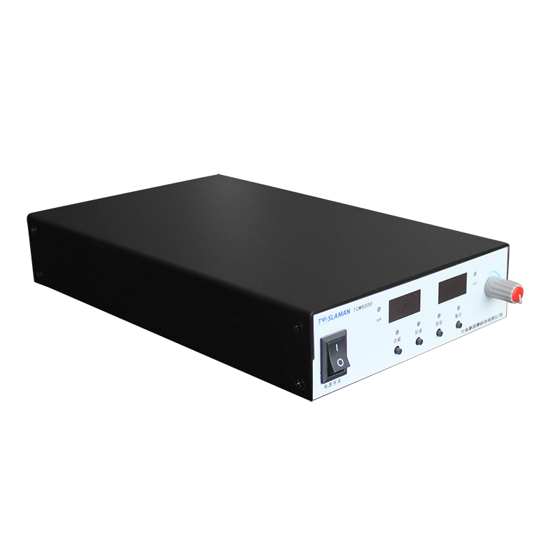
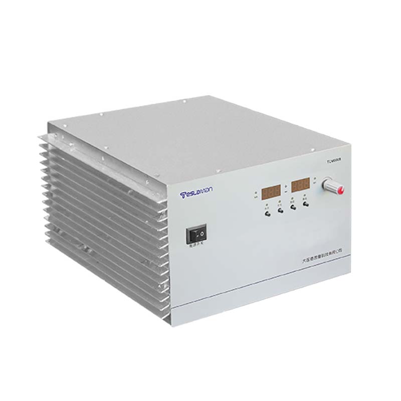
The power supply architecture for pulse shaping must meet demanding requirements. The RF generator must be capable of rapid amplitude modulation with precise control of the pulse shape. The matching network must maintain impedance matching during the pulse transitions to minimize reflected power. The bias measurement system must accurately capture the time-varying voltage and current waveforms. The control system must synchronize the pulse generation with the process timing requirements.
Fast rise and fall times in the pulse waveform enable sharp transitions between different ion energy regimes. During the rise time, the ion energy increases from zero to the peak value, with ions of intermediate energies bombarding the surface. A slow rise time results in a broader ion energy distribution, potentially causing unwanted etching at lower energies. Fast rise times concentrate the ion bombardment at the desired energy, improving selectivity and precision.
Pulse modulation techniques enable sophisticated control of the ion energy distribution. Amplitude modulation varies the pulse height to achieve different ion energies within a single process cycle. Frequency modulation changes the pulse repetition rate to control the average power and ion flux. Pulse width modulation adjusts the duty cycle to balance etching rate and selectivity. Combinations of these techniques can create complex pulse patterns optimized for specific etching applications.
The matching network presents particular challenges for pulsed operation. The plasma impedance changes during the pulse as the plasma density and sheath characteristics evolve. Traditional matching networks designed for continuous wave operation may not track these rapid impedance changes. Fast matching networks with active tuning can maintain optimal power transfer throughout the pulse duration. Alternatively, over-dimensioned matching networks can provide adequate matching over a range of plasma conditions.
Measurement and diagnostics are essential for optimizing pulse shaping parameters. Ion energy analyzers directly measure the ion energy distribution at the substrate surface. Optical emission spectroscopy monitors the plasma composition and excitation state. Voltage and current probes capture the electrical waveforms at the substrate electrode. Correlation of these measurements with etching results enables systematic optimization of the pulse parameters.
Process integration requires coordination between the bias power supply and other process equipment. The pulse timing must be synchronized with the gas flow switching that controls the surface modification steps. The pulse parameters may need to change between different phases of the atomic layer etching cycle. The control system must manage these transitions smoothly while maintaining process stability. Integration with the process chamber pressure control and temperature regulation ensures consistent etching conditions.
Reliability considerations affect the design of pulsed RF power supplies. The rapid switching of high power levels creates thermal cycling stress on components. The matching network components experience high voltages and currents during pulse transitions. The RF generator must maintain consistent pulse characteristics over millions of pulses. Component selection and thermal management ensure reliable operation over the equipment lifetime.