Advanced Electrostatic Chuck High Voltage Power Supply Precision Control Technology Research in Semiconductor Lithography Equipment
Electrostatic chucks in semiconductor lithography equipment require high voltage power supplies with exceptional precision control capabilities for reliable wafer handling during critical patterning processes. The electrostatic chuck provides mechanical clamping force through electrostatic attraction, eliminating mechanical clamping mechanisms that could damage delicate wafer surfaces or introduce particulate contamination. Precision control of the clamping voltage enables optimization of clamping force, thermal contact, and backside gas conductance for different process conditions and wafer types.
The fundamental operation of an electrostatic chuck involves application of high voltage to electrodes embedded within the chuck body, creating an electric field between the electrodes and the conductive wafer substrate. The electric field induces opposite charges on the wafer surface, generating electrostatic attraction force that holds the wafer against the chuck surface. The magnitude of the clamping force depends on the applied voltage, electrode geometry, dielectric layer thickness, and wafer resistivity.
Electrode configurations for electrostatic chucks include monopolar designs with a single electrode and bipolar designs with two electrodes of opposite polarity. Monopolar chucks require a conductive path from the wafer to ground for charge flow, typically provided by plasma in etch processes or by direct contact with a grounded chuck edge. Bipolar chucks generate clamping force through capacitive coupling between the two electrodes and the wafer, eliminating the need for wafer conductivity or external ground paths. Each configuration presents different requirements for power supply design and control.
Dielectric layer design for electrostatic chucks involves trade-offs between clamping force, dielectric strength, and thermal properties. Thinner dielectric layers provide higher clamping force for a given voltage but reduce the voltage margin before dielectric breakdown. Higher dielectric constant materials increase the capacitance and thus the clamping force, but may have inferior thermal properties for temperature control. Dielectric materials must maintain stable electrical properties over temperature ranges encountered during process operation and cleaning cycles.
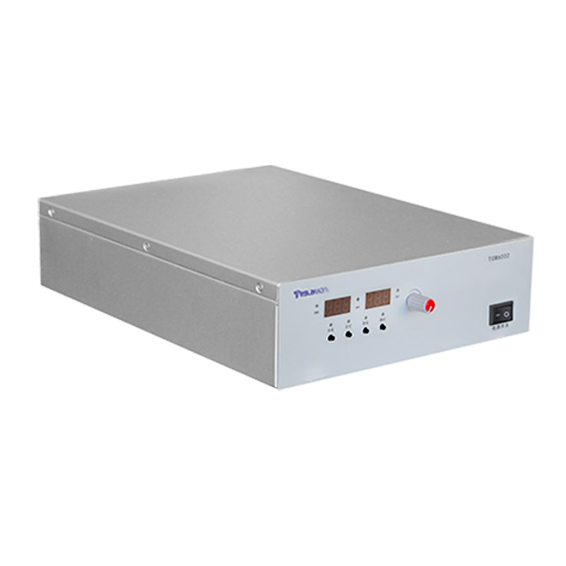
High voltage power supply requirements for electrostatic chucks include voltage range, current capability, ripple and noise, settling time, and control precision. Typical operating voltages range from 100 volts to several kilovolts, depending on chuck design and required clamping force. Current requirements are minimal during steady-state operation as the chuck behaves primarily as a capacitor. However, charging current during voltage changes and leakage current through the dielectric must be supplied. Voltage ripple and noise must be minimized to avoid fluctuations in clamping force that could affect wafer position during exposure.
Precision control of chuck voltage enables optimization for different process phases. Higher clamping force during wafer loading and unloading prevents wafer movement from handling forces. Reduced clamping force during thermal processes enables expansion and contraction of the wafer without inducing stress. Fine adjustment of voltage during exposure optimizes the balance between wafer stability and thermal contact resistance for temperature control. Voltage profiles for specific processes require programmable control with precise reproducibility.
Settling time for voltage changes affects throughput during process sequences that require voltage adjustment. Fast voltage ramps followed by rapid settling to the final value minimize transition time between process phases. The chuck capacitance, combined with power supply output impedance, determines the maximum charging rate. Power supply design for fast settling requires low output impedance and sufficient current capability to charge the chuck capacitance quickly.
Voltage measurement accuracy enables closed-loop control and monitoring of chuck condition. High voltage dividers scale the output voltage to levels suitable for measurement circuits. Divider accuracy and temperature stability affect voltage control precision. Calibration procedures establish the relationship between measured and actual voltage. Voltage monitoring during operation detects anomalies that could indicate dielectric degradation or contamination.
Current monitoring provides information about chuck leakage and condition. Leakage current through the dielectric indicates dielectric quality and contamination levels. Increasing leakage current over time may signal dielectric degradation requiring maintenance. Current monitoring during voltage changes indicates chuck capacitance, which can change with contamination or electrode degradation. Current measurement circuits with appropriate range and accuracy support condition monitoring and predictive maintenance.
Safety systems for electrostatic chuck power supplies include interlocks, discharge circuits, and ground fault detection. Interlocks prevent high voltage application when the chuck is not in a safe condition, such as when no wafer is present or when maintenance access doors are open. Discharge circuits rapidly remove stored charge from the chuck when voltage is removed, enabling safe wafer handling. Ground fault detection protects personnel and equipment from insulation failures that could energize exposed surfaces.
Integration with lithography equipment control systems enables coordinated operation of the chuck with other subsystems. Communication interfaces transmit voltage commands and receive status information. Sequence control coordinates voltage application with wafer handling, temperature control, and exposure operations. Data logging records voltage and current history for process traceability and condition monitoring.
Backside gas conductance between the wafer and chuck surface provides thermal contact for temperature control during processes that generate heat. The clamping force determines the degree of physical contact between wafer and chuck, affecting gas conductance and thermal resistance. Precision voltage control enables optimization of thermal contact for specific process requirements. Helium pressure in the backside gas channel affects thermal conductance independently of clamping force.
Wafer dechucking requires careful management to prevent wafer damage from residual electrostatic charge. Controlled voltage ramp-down allows charge dissipation through leakage paths. Active discharge circuits accelerate dechucking when faster wafer handling is required. The dechucking sequence must prevent sudden force release that could launch the wafer or cause it to stick to the chuck surface. Process development for dechucking optimizes speed while ensuring reliable wafer release.