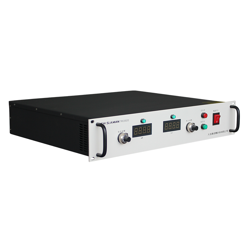
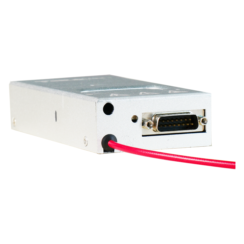
Power Control of Etch Equipment High-Voltage Supply in Self-Aligned Double Patterning
Self-aligned double patterning is a semiconductor manufacturing technique that doubles the pattern density of a layer by using a sacrificial spacer to define the final features. The technique involves multiple etch steps, each of which must remove the target material with a precisely controlled rate and profile. The etch equipment uses a plasma generated by a radio-frequency power source and a high-voltage bias that accelerates the ions toward the wafer. The high-voltage supply that provides the bias determines the ion energy and hence the etch rate, the selectivity, and the profile of the etched features.
The bias voltage is applied to the wafer electrode, and the voltage controls the energy with which the ions strike the wafer surface. The etch process requires a specific ion energy to achieve the desired etch rate and profile, and the bias supply must maintain this energy with a precision that is defined by the process. A variation of the bias voltage changes the etch rate and can cause the critical dimension of the features to deviate from the target. The supply therefore regulates the bias with a tight tolerance and a low ripple.
The etch process is controlled by the combination of the source power and the bias voltage. The source power determines the density of the plasma, and the bias voltage determines the ion energy. The process recipe specifies both parameters, and the etch tool controller adjusts the source power and the bias voltage according to the recipe. The bias supply accepts the setpoint from the controller and maintains the voltage with a response time that follows the recipe transitions without overshoot.
The self-aligned double patterning process is sensitive to the uniformity of the etch across the wafer. The etch rate varies with the position on the wafer, and the bias voltage contributes to this variation through the distribution of the plasma potential. The bias supply supports the uniformity by providing a stable voltage across the entire wafer, and the tool compensates for the residual non-uniformity by adjusting the process parameters. The bias voltage is measured at the wafer electrode, and the measured value is used in the process control.
The bias supply is a pulsed or continuous DC source depending on the etch chemistry and the tool design. In a pulsed bias configuration, the voltage is switched between two levels with a frequency and a duty cycle that are defined by the recipe. The pulse shape and the timing affect the ion energy distribution and the etch profile, and the supply must reproduce the pulse waveform with high fidelity. The pulse parameters are monitored, and any deviation from the recipe is reported to the tool controller.
Arc events occur in the etch chamber when the plasma becomes unstable or when a particle causes a local discharge. The arc can damage the wafer and the chamber components, and the bias supply must detect the arc and interrupt the bias within microseconds. The arc detection is based on the rapid change of the bias current, and the interruption prevents the arc energy from causing further damage. After the arc is extinguished, the supply restores the bias with a controlled sequence.
Long-term stability of the bias is essential for the run-to-run repeatability of the etch process. The supply is calibrated at defined intervals, and the drift of the output is monitored by the internal reference. The wafer-to-wafer variation of the etch results is tracked, and a correlation between the results and the bias measurements is used to identify any systematic drift. The maintenance is scheduled when the drift approaches the tolerance limit.
The bias supply communicates with the etch tool through a digital interface that carries the setpoints, the measured values, and the status. The tool controller manages the etch recipe and downloads the bias parameters to the supply at the start of each process step. The supply returns the actual voltage and current, and the values are logged for the process record. The communication is deterministic and supports the synchronization of the bias with the other process steps.
Reliability is a production requirement in a semiconductor fab. The cost of an unscheduled stop is very high, and the bias supply is designed with a high mean time between failures. The supply is equipped with redundant cooling, comprehensive diagnostics, and a monitoring system that predicts the end of life of the components. The spare modules are stocked, and the replacement is performed according to the documented procedures.
The supply is also designed for the cleanroom environment of the fab. The cabinet is sealed against particles, and the cooling air is filtered. The outgassing of the materials is controlled, and the supply is qualified for the cleanroom class of the etch bay. The acoustic noise is minimized to meet the noise budget of the fab.
Process development for a new etch step begins with a series of experiments that vary the bias parameters and measure the resulting etch profile. The experiments define the process window, and the bias supply is operated within this window for the production runs. The recorded bias parameters provide the evidence for the process qualification and for the ongoing process monitoring.
Safety interlocks protect the etch tool and the operator during the operation. The bias supply is interlocked with the chamber door, the vacuum status, and the plasma ignition state, and the high voltage is enabled only when all interlock conditions are satisfied. The stored energy of the output is discharged automatically when the process step ends, and the discharge time is documented. The interlock chain is tested at defined intervals, and the test results are recorded in the equipment log. The interlock design follows the principle that a failure of the interlock system must result in a safe state, so the supply defaults to the de-energized condition whenever the safety conditions cannot be confirmed.
In summary, the etch equipment high-voltage bias supply for self-aligned double patterning integrates precise voltage regulation, fast arc response, pulse waveform fidelity, and comprehensive diagnostics into a production-grade module. The result is a supply that maintains the ion energy control required for the accurate etching of the patterned features while supporting the automated operation of the etch tool. Every improvement in the bias stability, every refinement of the arc protection, and every enhancement of the process integration contributes directly to the yield and the precision of the manufactured devices. The engineering effort continues as double patterning extends to more complex integration schemes.