


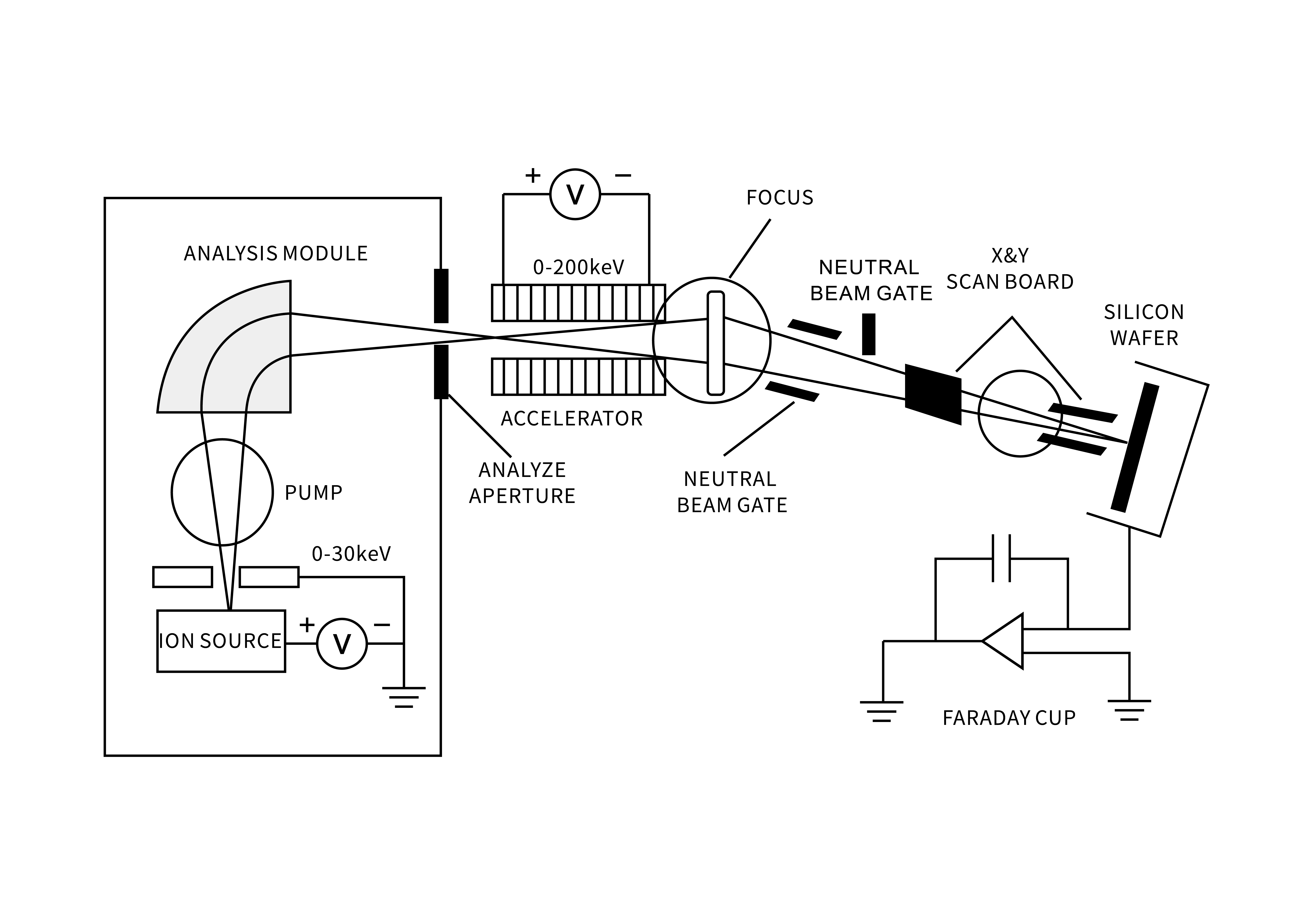
Ion implantation
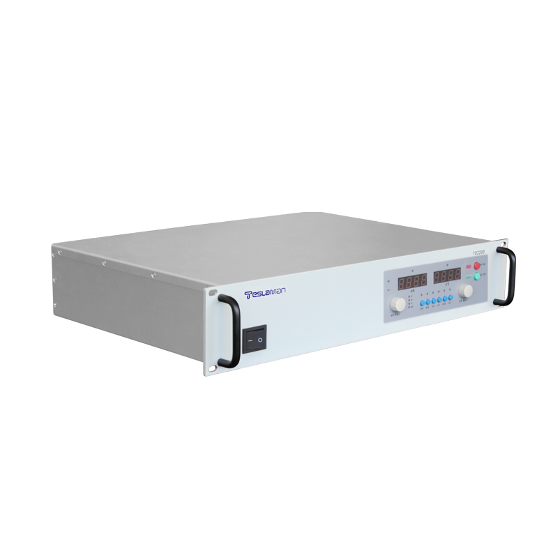
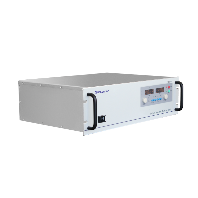
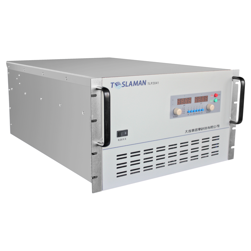
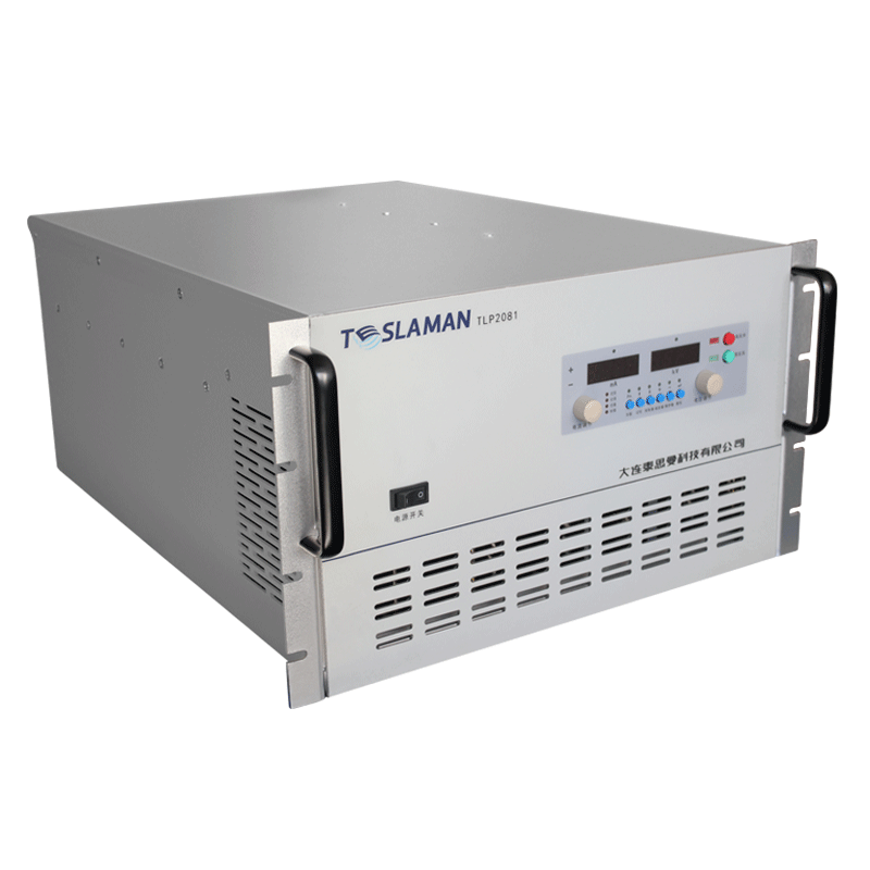
Ultra-high stability ultra-low ripple overvoltage overcurrent short circuit arc and overtemperature reliable protection
Ion implantation is a technology that accelerates charged ions (such as boron, phosphorus, etc.) into high-energy ion beams through-voltage power supply and precisely bombards the surface of materials (such as silicon wafers, metals, or ceramics) to change the physical and chemical properties of the surface. In semiconductor manufacturing, it achieves controllable doping of key structures such as the transistor's leakage area and well area by injecting specific impurity atoms into the silicon wafer; the field of materials, it can enhance the hardness of tools or the performance of optical devices. The core advantage of this technology lies in the highly precise control of doping depth,, and area, which is a key process for microelectronic chips and advanced material modification