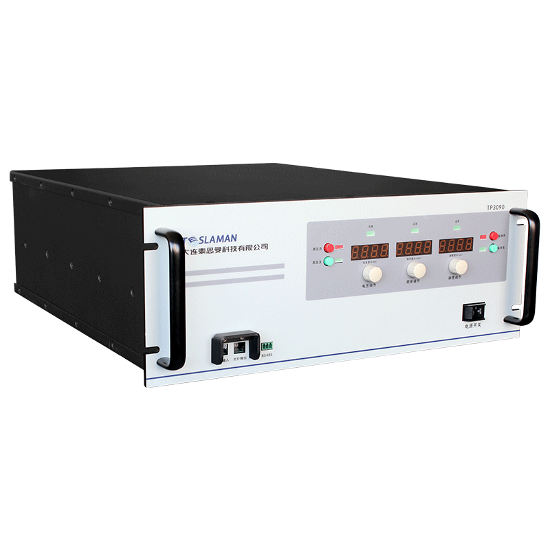
High-Voltage Control for Multi-Signal Synchronous Acquisition in Scanning Electron Microscopy
Modern scanning electron microscopes (SEMs) are multi-modal analytical platforms, capable of simultaneously generating secondary electron (SE), backscattered electron (BSE), and various X-ray signals for correlative analysis. The temporal and spatial synchronization of these disparate signals is critical for constructing accurate, pixel-registered multi-channel images. The high-voltage subsystems governing electron beam generation, scanning, and detection play an underappreciated yet central role in orchestrating this synchronous acquisition.
The primary high-voltage supply for the electron gun, typically ranging from 1 kV to 30 kV, sets the fundamental beam energy. Its stability directly impacts signal generation efficiency and spatial resolution. However, for synchronous acquisition, the critical requirement is the precise temporal relationship between the beam position and the sampling of each detector's output. The beam scanning is controlled by waveform generators driving high-voltage amplifiers attached to the deflection coils. These scan amplifiers must have exceptionally low phase distortion and group delay across their operating bandwidth. Any differential delay between the X and Y scan signals, or a time lag between the commanded scan position and the actual beam position, will cause misregistration between the SE image and the slower, time-integrated X-ray elemental map.
The synchronization challenge intensifies when using pulse-based techniques or in-situ experiments. For example, electron beam induced current (EBIC) or cathodoluminescence (CL) measurements may involve gating a detector or spectrometer based on beam blanking. The blanking system uses a pair of electrostatic plates driven by a high-voltage amplifier to deflect the beam off-axis rapidly. The timing jitter of this blanking amplifier's output transition directly translates into uncertainty in the exposure time per pixel for time-resolved signals. To achieve nanosecond-scale synchronization, the master clock for the entire SEM—governing scan generation, blanking, frame grabbers, and spectrometer triggering—is often derived from a single low-jitter oscillator. All high-voltage control modules, including the gun bias modulator, scan amps, and blanking amp, must accept and adhere to timing references from this central clock via deterministic digital interfaces.
Detector biasing itself requires synchronized high-voltage control. A photomultiplier tube (PMT) for CL detection or an active bias on a solid-state BSE detector may need its gain modulated in sync with the beam scan. For instance, when scanning from a region of a sample with high average atomic number to a low-Z region, the BSE yield changes dramatically. To prevent signal saturation or loss of contrast, the detector bias voltage can be automatically adjusted on a line-by-line or even pixel-by-pixel basis based on a pre-scan or a fast feedback loop. This requires a high-voltage output channel with a combination of fast switching speed and analog programmability, tightly slaved to the scan waveform.
Furthermore, advanced phase mapping or strain analysis techniques using electron backscatter diffraction (EBSD) require the beam to be rocked at high frequency over a few pixels to improve pattern quality. This rocking is achieved by adding a small, high-frequency oscillation to the standard scan waveforms. The high-voltage scan amplifiers must have the slew rate and bandwidth to superimpose this high-frequency component without distorting the primary raster, ensuring the diffraction patterns are collected from precisely known and controlled beam incidence angles relative to the primary scan coordinates.
Data acquisition in such a system is a orchestrated flow. At each pixel dwell time, defined by the master clock, the beam is at a known (X,Y) position. The control system simultaneously samples the analog outputs from the SE, BSE, and possibly multiple X-ray or current detectors. The high-voltage controllers for scan, blanking, and detector bias contribute timestamps or status flags to this data packet. Any latency or variability in the high-voltage systems' response becomes embedded as spatial blur or registration error in the final correlated dataset. Therefore, the design of these power supplies emphasizes not just stability and low noise, but also deterministic latency and extensive built-in diagnostic capabilities to verify timing alignment, ensuring that a chemical signal from an X-ray detector can be mapped with confidence onto the topographical detail revealed by secondary electrons.